This topic describes the front and rear-panel connectors for the M9384B VXGand the front-panel connectors for the M9383B VXG-m.
|
Connector |
Type |
Description |
|---|---|---|
|
DisplayPort |
DisplayPort |
For external display devices. Display Port Dual Mode DisplayPort++ (DVI-D, VGA, HDMI with an adapter). NOTE: To duplicate the instrument’s application on an external display it is recommended to set the resolution to 1280x768. |
|
USB 3.0 |
USB Type-A female |
Host controller, SuperSpeed, 900 mA (nominal) |
|
USB 2.0 High Power |
USB Type-A female |
Host controller, high-speed, 1.2 A (nominal) |
|
Ctrl S |
uHDMI female |
Reserved for future use. Damage level is ≤ 0.5 V and > 6.5 V. |
|
Ctrl M |
uHDMI female |
Reserved for future use. Damage level is ≤ 0.5 V and > 6.5 V. |
|
Ch 1 I+ In |
SMA female |
For Option EXT, externally supplied analog in-phase component of I/Q modulation to channel 1’s internal baseband generator. Frequency range is DC to 1000 MHz (nominal). 50 Ω impedance (nominal). Damage level is 5 Vpeak, 1 Vrms. |
|
Ch 1 I- In |
SMA female |
For Option EXT, externally supplied analog in-phase component of I/Q modulation to channel 1’s internal baseband generator, 180° out of phase from I+ In. Frequency range is DC to 1000 MHz (nominal). 50 Ω impedance (nominal). Damage level is 5 Vpeak, 1 Vrms. |
|
Ch 1 Q+ In |
SMA female |
For Option EXT, externally supplied analog quadrature-phase component of I/Q modulation to channel 1’s internal baseband generator. Frequency range is DC to 1000 MHz (nominal). 50 Ω impedance (nominal). Damage level is 5 Vpeak, 1 Vrms. |
|
Ch 1 Q- In |
SMA female |
For Option EXT, externally supplied analog quadrature-phase component of I/Q modulation to channel 1’s internal baseband generator, 180° out of phase from Q+ In. Frequency range is DC to 1000 MHz (nominal). 50 Ω impedance (nominal). Damage level is 5 Vpeak, 1 Vrms. |
|
Ch 2 I In |
SMA female |
For Option EXT and Option 002, input for in-phase component of channel 2’s analog I/Q modulation. Frequency range is DC to 1000 MHz (nominal). 50 Ω impedance (nominal). Damage level is 5 Vpeak, 1 Vrms. |
|
Ch 2 Q In |
SMA female |
For Option EXT and Option 002, input for quadrature component of channel 2’s analog I/Q modulation. Frequency range is DC to 1000 MHz (nominal). 50 Ω impedance (nominal). Damage level is 5 Vpeak, 1 Vrms. |
|
Ch 2 I Out |
SMA female |
For instruments with Option 002, outputs the in-phase component of channel 2’s analog I/Q modulation. Frequency range is DC to 1000 MHz (nominal). 50 Ω impedance (nominal). Damage level is ±2 V. |
|
Ch 2 Q Out |
SMA female |
For instruments with Option 002, outputs the quadrature component of channel 2’s analog I/Q modulation. Frequency range is DC to 1000 MHz (nominal). 50 Ω impedance (nominal). Damage level is ±2 V. |
|
Connector |
Type |
Description |
|---|---|---|
|
AM In |
BNC female |
Reserved for future use. For Option 303 externally provided AM modulation signal. 0 to 1 MHz (nominal). 1.0 V (nominal) for 100% AM. 1 MΩ impedance (nominal). Damage level is ±15 V. Instruments with Option 002 have connector for CH2. |
|
Pulse In |
BNC female |
For Options PME/PMR externally provided Pulse modulation signal. 1 MΩ impedance (nominal). Damage level is 10 Vpeak, 5 Vrms. Instruments with Option 002 have connector for CH2. |
|
LF1 Out |
SMB male |
Reserved for future use. 50 Ω impedance (nominal). Damage level is 10 Vpeak, 5 Vrms. Instruments with Option 002 have connector for CH2. |
|
Pulse Video Out |
SMB male |
For Options F32/F44 with Options PME/PMR, outputs signal following envelope of RF pulse. VOL < 0.4 V, VOH is 2.8 V to 3.3 V into high impedance. 50 Ω impedance (nominal). Damage level is ±5 V. Instruments with Option 002 have connector for CH2. |
|
Pulse Sync Out |
SMB male |
For Options F32/F44 with Options PME/PMR, outputs signal (trigger) related to pulse timing. VOL < 0.4 V, VOH is 2.8 V to 3.3 V into high impedance. 50 Ω impedance (nominal). Damage level is ±5 V. Instruments with Option 002 have connector for CH2. |
|
Trig 1 |
SMB male |
For Options F32/F44, reserved for future use. For Options F14/F20 with Options PME/PMR Pulse Video Out outputs signal following envelope of RF pulse. Instruments with Option 002 have connector for CH2. |
|
Trig 2 |
SMB male |
For Options F32/F44, reserved for future use. For Options F14/F20 with Options PME/PMR Pulse Sync Out outputs signal (trigger) related to pulse timing. VOL < 0.4 V, VOH is 2.8 V to 3.3 V into high impedance. 50 Ω impedance (nominal). Damage level is ±5 V. Instruments with Option 002 have connector for CH2. |
|
Settled |
SMB male |
Output signal to determine when the signal level is settled: logic High while settled and low (approximately 0 V) when change is in progress. CMOS +3.3 V Logic. Damage level is ≤ 0.5 V and > 6.5 V. Instruments with Option 002 have connector for CH2. |
|
100 MHz Out |
SMB male |
Output of 100 MHz CW frequency reference, switched from the user interface; off by default. High impedance when off, 50 Ω when on, level is +15 dBm (nominal). |
|
EFC In |
SMB male |
Reserved for future use. ESD damage level is 30 V. |
|
Ch 1 +I Out |
SMA female |
Analog in-phase component of I/Q modulation from channel 1’s internal baseband generator. Frequency range is DC to 1000 MHz (nominal). 50 Ω impedance (nominal). Damage level is ±2 V. |
|
Ch 1 -I Out |
SMA female |
Analog in-phase component of I/Q modulation from channel 1’s internal baseband generator, 180° out of phase from +I Out. Frequency range is DC to 1000 MHz (nominal). 50 Ω impedance (nominal). Damage level is ±2 V. |
|
Ch 1 +Q Out |
SMA female |
Analog quadrature-phase component of I/Q modulation from channel 1’s internal baseband generator. Frequency range is DC to 1000 MHz (nominal). 50 Ω impedance (nominal). Damage level is ±2 V. |
|
Ch 1 -Q Out |
SMA female |
Analog quadrature-phase component of I/Q modulation from channel 1’s internal baseband generator, 180° out of phase from +Q Out. Frequency range is DC to 1000 MHz (nominal). 50 Ω impedance (nominal). Damage level is ±2 V. |
|
RF Out |
Option F32/F44 - 2.4 mm male Option F14/F20 – APC 3.5 mm male |
RF Output signal, level selected by user interface. 50 Ω impedance (nominal). Instruments with Option 002 have connector for CH2. |
|
19.2 GHz Out 1 |
SMA female |
Output of 19.2 GHz CW frequency reference, cabled from the factory to 19.2 GHz In. This port is always-on level is 7.3 dBm (nominal), if alternate 19.2 GHz In is provided this port should be terminated with 50 Ω load. |
|
19.2 GHz Out 2 |
SMA female |
Output of 19.2 GHz CW frequency reference, switched from user interface; off by default. High impedance when off, 50 Ω when on, level is 7.3 dBm (nominal). |
|
19.2 GHz In |
SMA female |
Input for 19.2 GHz CW frequency reference required for instrument operation. +5 dBm (nominal). 50 Ω impedance (nominal). Damage level is +20 dBm. |
|
BBG Sync |
SMA female |
Reserved for future use. In instruments with Option 002 this is a wired-or of the two channels. |
|
Connector |
Type |
Description |
|---|---|---|
|
LINE |
|
AC power receptacle, accepts 3-pronged AC power cord supplied with the instrument |
|
GPIB |
Micro-D 25-pin |
IEEE-488.2, 1987 with listen and talk. Use accessory Y1260A for GPIB cabling. |
|
LAN |
RJ-45 |
GbE 10/100/1000BASE-T Ethernet: the LAN supports DHCP, connection monitoring, dynamic hostname services, TCP/IP communication, TCP keep alive, and SCPI remote programming |
|
CH 1 EXT 1 |
BNC female |
External trigger input for channel 1. 10 kΩ input impedance (nominal). Damage level is ±5 V. |
|
CH 1 SYNC OUT |
BNC female |
Output of TTL High as assigned to Signal’s Marker Setup for channel 1. VOL < 0.4 V, VOH is 2.8 V to 3.3 V into high impedance. 50 Ω impedance (nominal). Damage level is ±5 V. |
|
CH 2 EXT 1 |
BNC female |
For instruments with Option 002, external trigger input for channel 2. 10 kΩ input impedance (nominal). Damage level is ±5 V. |
|
CH 2 SYNC OUT |
BNC female |
For instruments with Option 002, output of TTL High as assigned to Signal’s Marker Setup for channel 2. VOL < 0.4 V, VOH is 2.8 V to 3.3 V into high impedance. 50 Ω impedance (nominal). Damage level is ±5 V. |
|
10 MHz OUT |
BNC female |
Output of 10 MHz CW frequency reference, this port is always on. Serial numbers ≥ US/MY61260101: ≥ 5 dBm, 7 dBm (typical), square wave (See M9384BU-RUO.) Serial numbers < US/MY61260101: ≥ 10 dBm, 13 dBm (typical), sine wave 50 Ω impedance (nominal). ESD damage level is 30 V. |
|
10 MHz IN |
BNC female |
Externally supplied 10 MHz CW frequency reference, switched by the user interface; off by default. Input level -3 dBm to +20 dBm (nominal), 50 Ω impedance. ESD damage level is 30 V. |
|
100 MHz OUT |
SMA female |
Output of 100 MHz CW frequency reference, cabled from the factory to EXT CLK IN. This port is always-on level is +15 dBm (nominal). If alternate EXT CLK IN is provided this port should be terminated with 50 Ω load. Connector for CH1 and CH2. |
|
EXT CLK IN |
SMA female |
Input of an external 100 MHz reference clock required for instrument operation. +10 dBm (nominal). 50 Ω impedance (nominal). Damage level is +20 dBm. One per channel, channel 2 is unused if Option 002 is not present. |
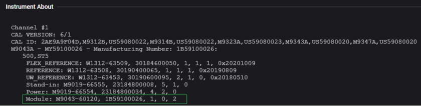
Reference Output Coherency upgrade (M9384BU-RUO) can be identified by checking the Chronos HWID. Click or tap the System Menu > Settings > Instrument Information > Instrument About. If this modification has been performed, you will see "Module: M9043-60120, XXXXXXXXXX, X, X, 2."
|
Module |
Connector |
Type |
Description |
|---|---|---|---|
|
M9037A |
GPIB |
Micro-D 25-pin |
IEEE-488.2, 1987 with listen and talk. Use accessory Y1260A for GPIB cabling. |
|
M9037A |
LAN 1 |
RJ45 Ethertwist |
GbE 10/100/1000BASE-T Ethernet: the LAN supports DHCP, connection monitoring, dynamic hostname services, TCP/IP communication, TCP keep alive, and SCPI remote programming |
|
M9037A |
DisplayPort |
DisplayPort |
For external display devices. Display Port Dual Mode DisplayPort++ (DVI-D, VGA, HDMI with an adapter). NOTE: To duplicate the instrument’s application on an external display it is recommended to set the resolution to 1280x768. |
|
M9037A |
USB 3.0 |
USB Type-A female |
Host controller, SuperSpeed, 900 mA (nominal) |
|
M9037A |
USB 2.0 |
USB Type-A female |
Host controller, high-speed |
|
M9043A |
HF Out 1 |
SMA (f) |
Output of 19.2 GHz CW frequency reference, switched from user interface; off by default. High impedance when off, 50 Ω when on, level is 7.3 dBm (nominal). |
|
M9043A |
Trig 1 |
SMB (m) |
For Options F32/F44, reserved for future use. For Options F14/F20 with Options PME/PMR Pulse Video Out outputs signal following envelope of RF pulse. |
|
M9043A |
Trig 2 |
SMB (m) |
For Options F32/F44, reserved for future use. For Options F14/F20 with Options PME/PMR and Option 002, channel 2's Pulse Video Out outputs signal following envelope of RF pulse. |
|
M9043A |
Ref In |
SMB (m) |
Externally supplied 10 MHz CW frequency reference, switched by the user interface; off by default. NOTE: when using an external frequency reference this connector is preferred over the M9043A Rear Panel 10 MHz IN. Input level -3 dBm to +20 dBm (nominal), 50 Ω impedance. ESD damage level is 30 V. |
|
M9043A |
EFC/Cal In |
SMB (m) |
Reserved for future use. ESD damage level is 30 V. |
|
M9043A |
OCXO/Cal Out |
SMB (m) |
Output of 10 MHz CW frequency reference, this port is always on. NOTE: when using the frequency reference to provide frequency lock with another instrument this connector is preferred over the M9043A Rear Panel 10 MHz OUT. +15 dBm (nominal). 50 Ω impedance (nominal). ESD damage level is 30 V. |
|
M9043A |
100 MHz Out 1 |
SMB (m) |
Output of 100 MHz CW frequency reference, cabled from the factory to M9343A Ext Clk In. This port is always-on level is +15 dBm (nominal). If alternate M9343A Ext Clk In is provided this port should be terminated with 50 Ω load. |
|
M9043A |
100 MHz Out 5 |
SMB (m) |
Output of 100 MHz CW frequency reference, switched from the user interface; off by default. High impedance when off, 50 Ω when on, level is +15 dBm (nominal). |
|
M9312B |
AM In |
SMP (m) |
Reserved for future use. For Option 303 externally provided AM modulation signal. 0 to 1 MHz (nominal). 1.0 V (nominal) for 100% AM. 1 MΩ impedance (nominal). Damage level is ±15 V. |
|
M9314B |
Trig 1 |
SMP (m) |
For Options PME/PMR externally provided Pulse modulation signal. 1 MΩ impedance (nominal). Damage level is 10 Vpeak, 5 Vrms. |
|
M9314B |
AM Out |
SMP (m) |
Reserved for future use. 50 Ω impedance (nominal). Damage level is 10 Vpeak, 5 Vrms. |
|
M9323A |
RF Out |
2.4 mm (f) |
For Options F32/F44 RF Output signal, level selected by user interface. 50 Ω impedance (nominal). |
|
M9323A |
Trig 1 |
SMP (m) |
For Options F32/F44 with Options PME/PMR, outputs signal following envelope of RF pulse. VOL < 0.4 V, VOH is 2.8 V to 3.3 V into high impedance. 50 Ω impedance (nominal). Damage level is ±5 V. |
|
M9323A |
Trig 2 |
SMP (m) |
For Options F32/F44 with Options PME/PMR, outputs signal (trigger) related to pulse timing. VOL < 0.4 V, VOH is 2.8 V to 3.3 V into high impedance. 50 Ω impedance (nominal). Damage level is ±5 V. |
|
M9343A |
RF 1 Out |
APC 3.5 mm (f) |
For Options F14/F20 RF Output signal, level selected by user interface. 50 Ω impedance (nominal). |
|
M9343A |
I+ Output |
SMP (m) |
Analog in-phase component of I/Q modulation from internal baseband generator. Frequency range is DC to 1000 MHz (nominal). 50 Ω impedance (nominal). Damage level is ±2 V. |
|
M9343A |
I- Output |
SMP (m) |
Analog in-phase component of I/Q modulation from internal baseband generator, 180° out of phase from +I Out. Frequency range is DC to 1000 MHz (nominal). 50 Ω impedance (nominal). Damage level is ±2 V. |
|
M9343A |
Q+ Output |
SMP (m) |
Analog quadrature-phase component of I/Q modulation from internal baseband generator. Frequency range is DC to 1000 MHz (nominal). 50 Ω impedance (nominal). Damage level is ±2 V. |
|
M9343A |
Q- Output |
SMP (m) |
Analog quadrature-phase component of I/Q modulation from internal baseband generator, 180° out of phase from +Q Out. Frequency range is DC to 1000 MHz (nominal). 50 Ω impedance (nominal). Damage level is ±2 V. |
|
M9343A |
I+ Input |
SMP (m) |
For Option EXT, externally supplied analog in-phase component of I/Q modulation to internal baseband generator. Frequency range is DC to 1000 MHz (nominal). 50 Ω impedance (nominal). Damage level is 5 Vpeak, 1 Vrms. |
|
M9343A |
I- Input |
SMP (m) |
For Option EXT, externally supplied analog in-phase component of I/Q modulation to internal baseband generator, 180° out of phase from I+ In. Frequency range is DC to 1000 MHz (nominal). 50 Ω impedance (nominal). Damage level is 5 Vpeak, 1 Vrms. |
|
M9343A |
Q+ Input |
SMP (m) |
For Option EXT, externally supplied analog quadrature-phase component of I/Q modulation to internal baseband generator. Frequency range is DC to 1000 MHz (nominal). 50 Ω impedance (nominal). Damage level is 5 Vpeak, 1 Vrms. |
|
M9343A |
Q- Input |
SMP (m) |
For Option EXT, externally supplied analog quadrature-phase component of I/Q modulation to internal baseband generator, 180° out of phase from Q+ In. Frequency range is DC to 1000 MHz (nominal). 50 Ω impedance (nominal). Damage level is 5 Vpeak, 1 Vrms. |
|
M9343A |
Trig 1 |
SMP (m) |
Output of TTL High as assigned to Signal’s Marker Setup. VOL < 0.4 V, VOH is 2.8 V to 3.3 V into high impedance. 50 Ω impedance (nominal). Damage level is ±5 V. |
|
M9343A |
Trig 2 |
SMP (m) |
For Options F32/F44, reserved for future use. For Options F14/F20 with Options PME/PMR Pulse Sync Out outputs signal (trigger) related to pulse timing. VOL < 0.4 V, VOH is 2.8 V to 3.3 V into high impedance. 50 Ω impedance (nominal). Damage level is ±5 V. |
|
M9343A |
Sync (upper left) |
SMP (m) |
Reserved for future use. |
|
M9343A |
Ext 1 |
SMP (m) |
External trigger input. 10 kΩ input impedance (nominal). Damage level is ±5 V. |
|
M9343A |
USB |
|
Reserved for future use. Not for use with USB devices. |
|
M9347A |
Mark 1 |
SMP (m) |
Output signal to determine when the signal level is settled: logic High while settled and low (approximately 0 V) when change is in progress. CMOS +3.3 V Logic. Damage level is ≤ 0.5 V and > 6.5 V. |
|
M9347A |
Mark 2 |
SMP (m) |
For instruments with Option 002, channel 2's output signal to determine when the signal level is settled: logic High while settled and low (approximately 0 V) when change is in progress. CMOS +3.3 V Logic. Damage level is ≤ 0.5 V and > 6.5 V. |
|
M9347A |
Ctrl M |
uHDMI (f) |
Reserved for future use. Damage level is ≤ 0.5 V and > 6.5 V. |
|
M9347A |
Ctrl S |
uHDMI (f) |
Reserved for future use. Damage level is ≤ 0.5 V and > 6.5 V. |
|
Rear Panel |
10 MHz OUT |
BNC female |
Output of 10 MHz CW frequency reference, this port is always on. Serial numbers ≥ MY61300101: ≥ 5 dBm, 7 dBm (typical), square wave (See M9384BU-RUO.) Serial numbers < MY61300101: ≥ 10 dBm, 13 dBm (typical), sine wave 50 Ω impedance (nominal). ESD damage level is 30 V. |